
 BETA
BETA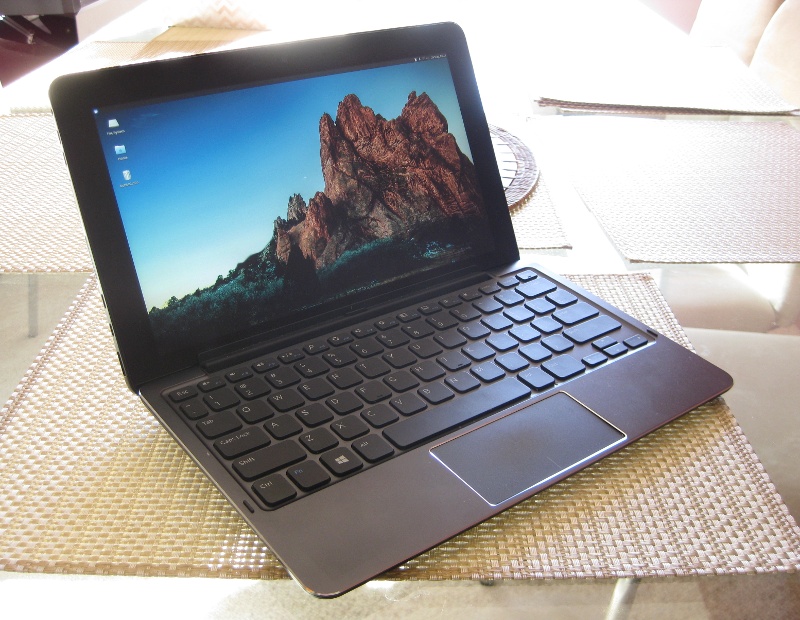
Introduction
I recently purchased a pair of Dell Venue 11 Pro 7140 tablet computers — one for myself and one for my girlfriend. I figured this would be a good crossover device between a tablet and a laptop, and so far I’m not disappointed. One important reason I chose this model is because they are more easily serviceable than other comparable offerings like the Microsoft Surface Pro line; the Surface Pro is glued together in a way that is difficult to disassemble and reassemble, which makes me very unhappy. Batteries have a limited service life (as I know all too well from my last post), and I don’t want to throw away a perfectly good tablet in a couple of years just because the battery is not holding a charge. Even if you don’t have any interest in taking apart your own devices, I would encourage you to consider the fixability of your device and vote with your wallet against throw-away devices. Anyway, enough of that rant.
Together with my Dell tablet I bought a keyboard. There’s two types of keyboard available for the Dell Venue 11 Pro: a “slim tablet” keyboard (K11A), which is just a keyboard and touchpad, and a “mobile” or “travel” keyboard (K12A), which additionally has a battery in it. I chose the latter version with the battery inside so that I could get more battery life out of my tablet.
I ran into an interesting problem with the travel keyboard, or at least my unit. Sometimes after attaching it to the tablet, the touchpad didn’t work. Sometimes the whole keyboard wouldn’t work. Strangely though, if I disconnected the battery inside the keyboard or let it drain completely, it would always work reliably, so I knew that it was some interaction with the voltage from the battery.
Most people at this point would call Dell, and unless you’re an electronics geek this is probably the best option. But I thought I would try to track it down.
Initial probing
The first thing I did after removing the cover was to probe the 6-pin touchpad connector, since that was the most obvious point of brokenness. The pinout for this connector looks approximately like this:
| Pin | Description |
|---|---|
| 1 | I/O (PS/2 clock?) |
| 2 | ground |
| 3 | I/O (PS/2 data?) |
| 4 | connected to 3.3V via 0 ohm jumper |
| 5 | I/O (touchpad button?) |
| 6 | 3.3V |
In normal working operation, five of the six pins — all except ground — probed as 3.3V, which is the normal idle state of the PS/2 bus. In the broken state, pin 3 was stuck low (0V). Essentially the touchpad PS/2 bus was in a locked up state. Note that the button may still work in this state (as I recall someone else on the Internet noting).
Most interesting was what happened when the keyboard was disconnected from the tablet, leaving it powered only by its internal battery. Now all the 3.3V pins dropped to 2V. This was likely the cause of the PS/2 bus lockups: the components running off that voltage supply (touchpad, keyboard, and associated microcontroller) were unlikely to work reliably at 2V. When the tablet was plugged back in, the voltage rose back to 3.3V, but the microcontroller and/or touchpad were sometimes in a bad state from their sojourn at 2V.
I initially thought that that the 2V might be due to a “back powering” issue (“back powering” occurs when an unpowered IC has voltage applied to some I/O pins, and current flows from those I/O pins into the power rail). However, I couldn’t find any ICs that were connected in a way that would cause back-powering. Rather it seemed that there was some issue with the circuit that turns the power on and off.
Power control circuit
The circuit that controls power to the keyboard/touchpad looks like this:
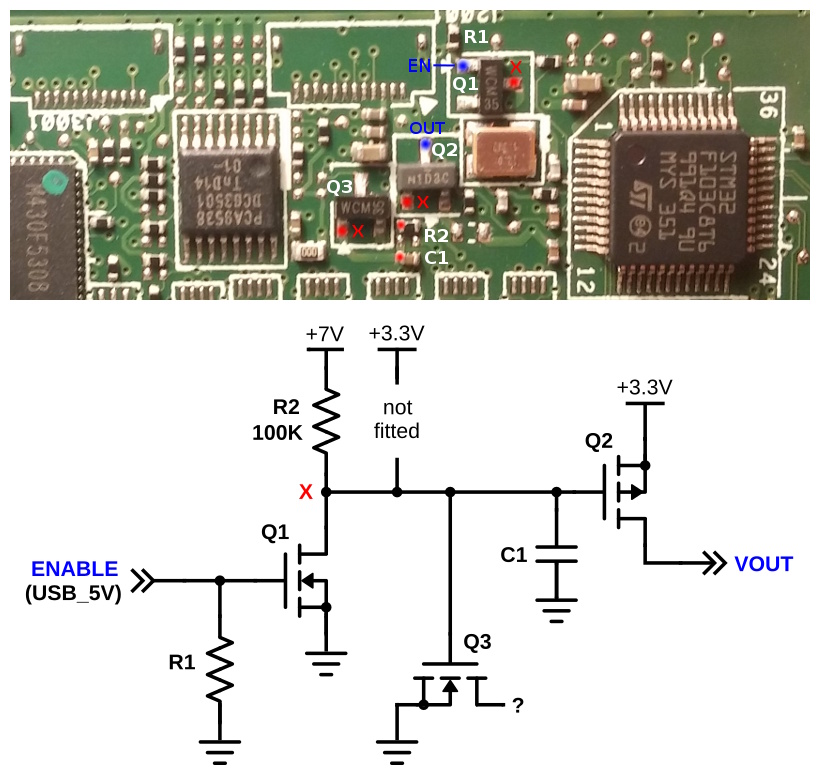
This type of circuit is what’s known as a “high-side switch”. The element doing the actual switching is Q2, a P-channel MOSFET transistor, and Q1 is an N-channel MOSFET acting (together with R2) as an inverter.
When the keyboard is attached to the tablet, ENABLE (USB_5V) is 5V → transistor Q1 is on → node X is pulled to ground → Q2 turns on fully → OUT is 3.3V. This was working as expected in my keyboard.
When the keyboard is disconnected, USB_5V is floating and pulled down to ground by R1 → Q1 is off → node X should be pulled up to 7V by R2 → Q2 should turn off fully → OUT should float to 0V assuming nothing else is powering it. This was not working correctly in my unit. Instead, node X was at 2.7V and OUT at 2.0V.
(N.B. the “7V” I refer to may not be exactly 7V; it’s the battery voltage minus a bit so may be higher or lower depending on how much charge is in the battery.)
Tracking down the problem
My first thought was that the 100K pull-up resistor might be too high, and the leakage current through the three transistors was dragging down node X from 7V to 2.7V (it only takes 40 μA to drop 4V across 100K, and in my world 40 μA is tiny).
I removed R1 from the board and replaced it with a 65K resistor instead, thinking that would solve the problem. To my great surprise node X remained around 2.7V.
I then tried temporarily connecting node X to 3.3V with a 10K resistor to make the pull-up even stronger, and it still barely moved above 2.7V.
The value 2.7V is about a diode drop below 3.3V which I thought might be a clue. To determine whether this was relevant, I tried an experiment with the 3.3V rail off, connecting node X to 2V from a current-limited power supply. Now both the 3.3V rail and the OUT rail were hovering at 1.2V, and node X was sinking about 1.2mA. Where was this current going? Q1 should have been off, and Q2 and Q3 are oriented with their gates connected to node X so should not be sinking any current from it (the gate of a MOSFET is insulated from the other terminals so the gate current should be essentially zero).
I considered three options:
- Q2 was not a P-channel MOSFET but something else. (I couldn’t determine the part number for any of Q1/Q2/Q3; part markings on these tiny SMD parts often have no correlation with the part numbers, so working backwards from markings is difficult unless you happen to stumble on the right datasheet.)
- There was something else connected to node X that I hadn’t found in my tracing of the board.
- One of the transistors was broken and leaking current.
Testing components in-situ is tricky as multimeter readings are affected by anything else connected to the nodes, for example node X has a capacitor that will sink current until charged up. After a day of head-scratching and verifying my schematic, I decided that (c) was most likely and I pulled Q2 off the circuit board with a dose of hot air.
It was immediately apparent that Q2 was broken as its gate-to-source and gate-to-drain resistances were only a few kiloohms. In a MOSFET, the gate is behind an insulator, so these resistances should be megaohms. The low resistance from gate-to-source and gate-to-drain suggests that the gate oxide in this MOSFET is damaged. (Interestingly, the resistance is different in the gate-to-source direction vs the source-to-gate direction, and similarly for gate-to-drain vs drain-to-gate. This makes sense if you consider that a MOSFET, under the oxide, contains two p-n junctions like a BJT transistor.)
After replacing Q2 with a new P-channel MOSFET, the output voltage now turns off fully, and my keyboard and touchpad work normally.
Final thoughts
One thing I learnt from this debugging process is that MOSFETs can fail in interesting ways: not just ‘on’ or ‘off’, but with current leaks that behave partly like resistors and partly like p-n junctions, reflecting the internal construction of the device.
As to why this device failed, I’m still not sure. My best guess from the marking (N1D3C) is that it’s an Si2301CDS which, if correct, seems perfectly up to the task. Most MOSFET power switches fail due to thermal stresses, but the current delivered by this circuit is very low compared to what this transistor can handle. I also doubt that there are any transient voltage spikes as both input and output have capacitors. My only thought is that the pull-up to around 7V (VGS(off) around +4V) may contribute to stress on the gate oxide over time, compared to if it was driven more conservatively with 3.3V (VGS(off) = 0V). The purpose of driving the gate to +4V when off is likely to reduce off-state power consumption, by “over pinching” the channel to reduce leakage. However it may also increase the likelihood of charge carriers migrating into the gate oxide. The datasheet specifies VGS = +8V as the “absolute maximum” beyond which permanent damage may occur, however there will also be a threshold beyond which device reliability is affected, which is unfortunately not stated in the datasheet. It may be that keeping the device for extended periods at VGS around +4V — as will be the case whenever the keyboard is off — is not a good idea. It’s clear that the designer wasn’t sure what the right answer was, either, since they’ve included pads for pulling up to both 3.3V and to 7V. Presumably a lot of people have this keyboard and it works just fine, so there is some element of silicon defects or bad luck as well.
Anecdotally it seems that a few other people on the Internet have had similar issues to mine, although I’m not sure whether they all stem from the same root cause. If you have this exact same behaviour (your Venue 11 Pro touchpad doesn’t work when the battery is charged but works reliably when battery is flat), and if you’re an electronics geek and you want to open your keyboard, I’d love to know whether your voltages at X and OUT have a similar anomaly to mine. Of course, if you can get it fixed under warranty then you should probably do that before risking voiding your warranty 🙂

Hey Matt,
Thanks for the story, I changed the one FET – and it worked like a charm!
The SI2301 CDS I could not get, so I used a SI2307CDS
SI2307CDS-T1-GE3
Tranzistor:P-MOSFET;unipolární;-30V;-2,2A;1,8W;SOT23
Výrobce: VISHAY Originální symbol: SI2307CDS-T1-GE3 RoHS
I’m in Europe, and used TME.EU to get the parts. Not even 10 cents / pcs and second-day delivery.
The smallest quantity I could order was 5 pcs – I glued the remaining 4 INSIDE the keyboard, should it stop working again I won’t have to search the mancave for those tiny, tiny parts.
Great detective job! i’ll be ordering soon.
$.51 @ https://www.mouser.com/ProductDetail/Vishay-Siliconix/SI2301CDS-T1-E3
I’ll let you know